The technological advancement of optical lenses has long been a significant marker of human scientific achievement. Eyeglasses, telescopes, cameras, and microscopes have all literally and figuratively allowed us to see the world in a new light. Lenses are also a fundamental component of manufacturing nanoelectronics by the semiconductor industry.
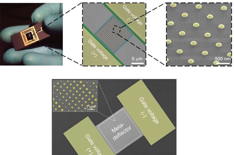
One of the most impactful breakthroughs of lens technology in recent history has been the development of photonic metasurfaces—artificially engineered nanoscale materials with remarkable optical properties. Georgia Tech researchers at the forefront of this technology have recently demonstrated the first-ever electrically tunable photonic metasurface platform in a recent study published by Nature Communications.
“Metasurfaces can make the optical systems very thin, and as they become easier to control and tune, you’ll soon find them in cell phone cameras and similar electronic imaging systems,” said Ali Adibi, professor in the School of Electrical and Computer Engineering at the Georgia Institute of Technology.
The pronounced tuning measures achieved through the new platform represent a critical advancement towards the development of miniaturized reconfigurable metasurfaces. The results of the study have shown a record eleven-fold change in the reflective properties, a large range of spectral tuning for operation, and much faster tuning speed.
Heating up metasurfaces
Metasurfaces are a class of nanophotonic materials in which a large range of miniaturized elements are engineered to affect the transmission and reflection of light at different frequencies in a controlled way.
“When viewing under very strong microscopes, metasurfaces look like a periodic array of posts,” said Adibi. “The best analogy would be to think of a LEGO pattern formed by connecting many similar LEGO bricks next to each other.”
Since their inception, metasurfaces have been used to demonstrate that very thin optical devices can affect light propagation with metalenses (the formation of thin lenses) being the most developed application.
Despite impressive progress, most demonstrated metasurfaces are passive, meaning their performance cannot be changed (or tuned) after fabrication. The work presented by Adibi and his team, led by Ph.D. candidate Sajjad Abdollahramezani, applies electrical heat to a special class of nanophotonic materials to create a platform that can enable reconfigurable metasurfaces to be easily manufactured with high levels of optical modulation.
PCMs provide the answer
A wide range of materials may be used to form metasurfaces, including metals, oxides, and semiconductors, but Abdollahramezani and Adibi’s research focuses on phase-change materials (PCMs) because they can form the most effective structures with the smallest feature sizes. PCMs are substances that absorb and release heat during the process of heating and cooling. They are called “phase-change” materials because they go from one crystallization state to another during the thermal cycling process. Water changing from a liquid to a solid or gas is the most common example.
The Georgia Tech team’s experiments are substantially more complicated than heating and freezing water. Knowing that the optical properties of PCMs can be altered by local heating, they have harnessed the full potential of the PCM alloy Ge2Sb2Te5 (GST), which is a compound of germanium, antimony, and tellurium.
By combining the optical design with a miniaturized electrical microheater underneath, the team can change the crystalline phase of the GST to make active tuning of the metasurface device possible. The fabricated metasurfaces were developed at Georgia Tech’s Institute for Electronics and Nanotechnology (IEN) and tested in characterization labs by illuminating the reconfigurable metasurfaces with laser light at different frequencies and measuring the properties of the reflected light in real time.
What tunable metasurfaces mean for the future
Driven by device miniaturization and system integration, as well as their ability to selectively reflect different colors of light, metasurfaces are rapidly replacing bulky optical assemblies of the past. Immediate impact on technologies like LiDAR systems for autonomous cars, imaging, spectroscopy, and sensing is expected.
With further development, more aggressive applications like computing, augmented reality, photonic chips for artificial intelligence, and biohazard detection can also be envisioned, according to Abdollahramezani and Adibi.
“As the platform continues to develop, reconfigurable metasurfaces will be found everywhere,” said Adibi. “They will even empower smaller endoscopes to go deep inside the body for better imaging and help medical sensors detect different biomarkers in blood.”
You may like to read:
For the first time, researchers have observed an X-ray explosion on a white dwarf
Study reveals corrosion of magnesium alloys in marine atmospheric environment


